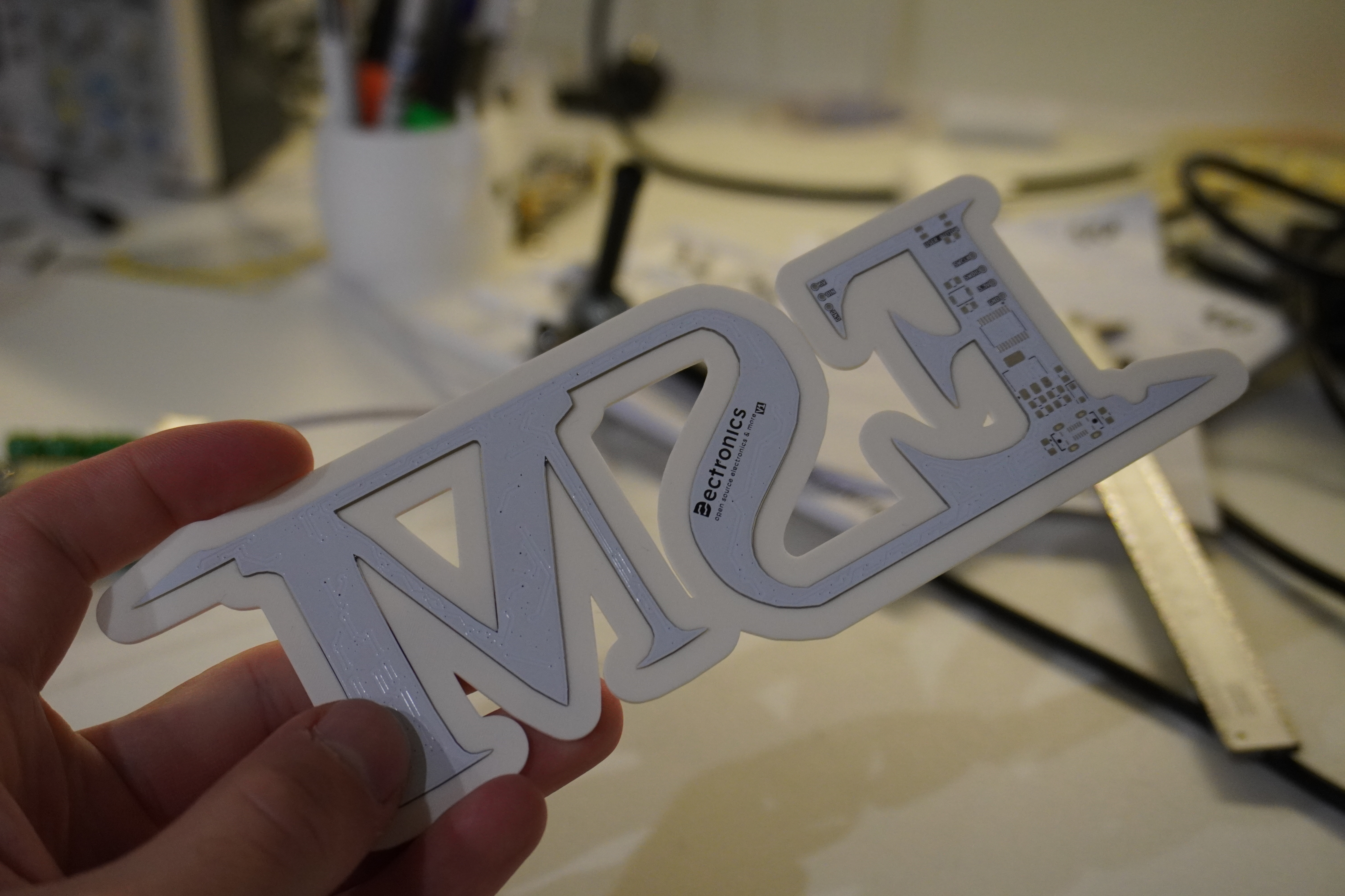
How good is kikit ?
I recently came across this plugin for KiCad that looked very cool.
 I always solder my SMD PCBs by exporting the board to .dxf in KiCad, importing it into Onshape, and then extruding it by 0.2 mm to get the layout. After that, I manually place it in the correct position.
Well, with KiKit all of this can be automated by simply giving the PCB to the editor, and it will also generate a nice border so the PCB is placed directly in the right spot — how handy!
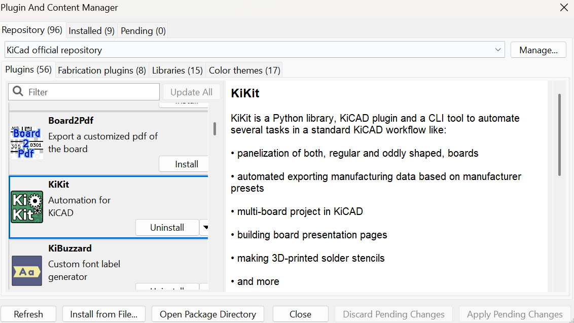
After quite a struggle to get it installed, I managed to get it working in the KiCad 9.0 Command Prompt.
To generate a custom 3D-printed stencil, I used this command:
I always solder my SMD PCBs by exporting the board to .dxf in KiCad, importing it into Onshape, and then extruding it by 0.2 mm to get the layout. After that, I manually place it in the correct position.
Well, with KiKit all of this can be automated by simply giving the PCB to the editor, and it will also generate a nice border so the PCB is placed directly in the right spot — how handy!
After quite a struggle to get it installed, I managed to get it working in the KiCad 9.0 Command Prompt.
To generate a custom 3D-printed stencil, I used this command:
"<PATH_TO_KIKIT>\kikit.exe" stencil createprinted ^
  --pcbthickness <PCB_THICKNESS_MM> ^
  --thickness <STENCIL_THICKNESS_MM> ^
  --framewidth <FRAME_WIDTH_MM> ^
  --frameclearance <FRAME_CLEARANCE_MM> ^
  --enlargeholes <ENLARGE_HOLES_MM> ^
  "<PATH_TO_PCB_FILE>.kicad_pcb" ^
  "<OUTPUT_FOLDER>"
I used these parameters for my test:
"C:\KiKit\kikit.exe" stencil createprinted ^
  --pcbthickness 1.6 ^
  --thickness 0.2 ^
  --framewidth 5 ^
  --frameclearance 0.1 ^
  --enlargeholes 0.1 ^
  "C:\Project\board.kicad_pcb" ^
  "C:\Project\stencils"
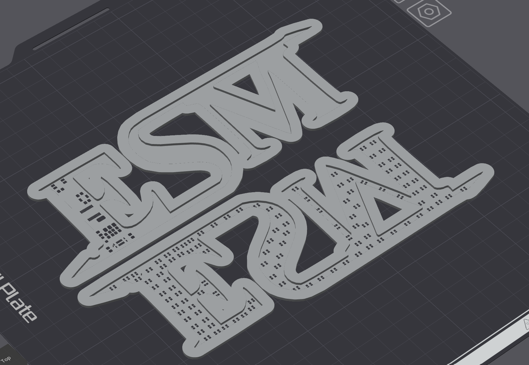
The output from this command looked very promising:
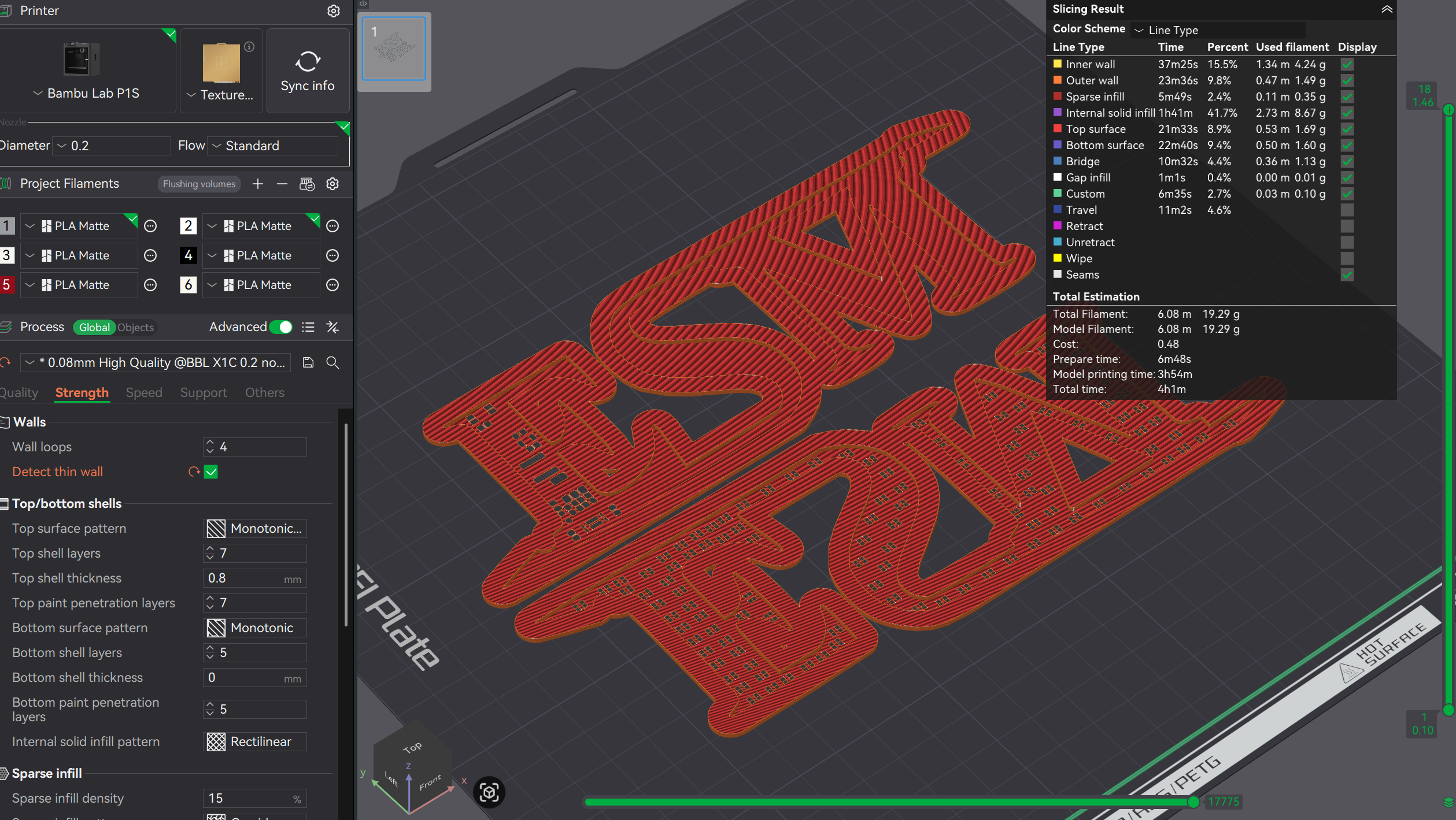
 I swapped the 0.4 mm nozzle on my P1S for a 0.2 mm nozzle to get more precision for the pad holes, and used these settings:
 After printing, it looked sooo cool and it was a perfect fit! (:
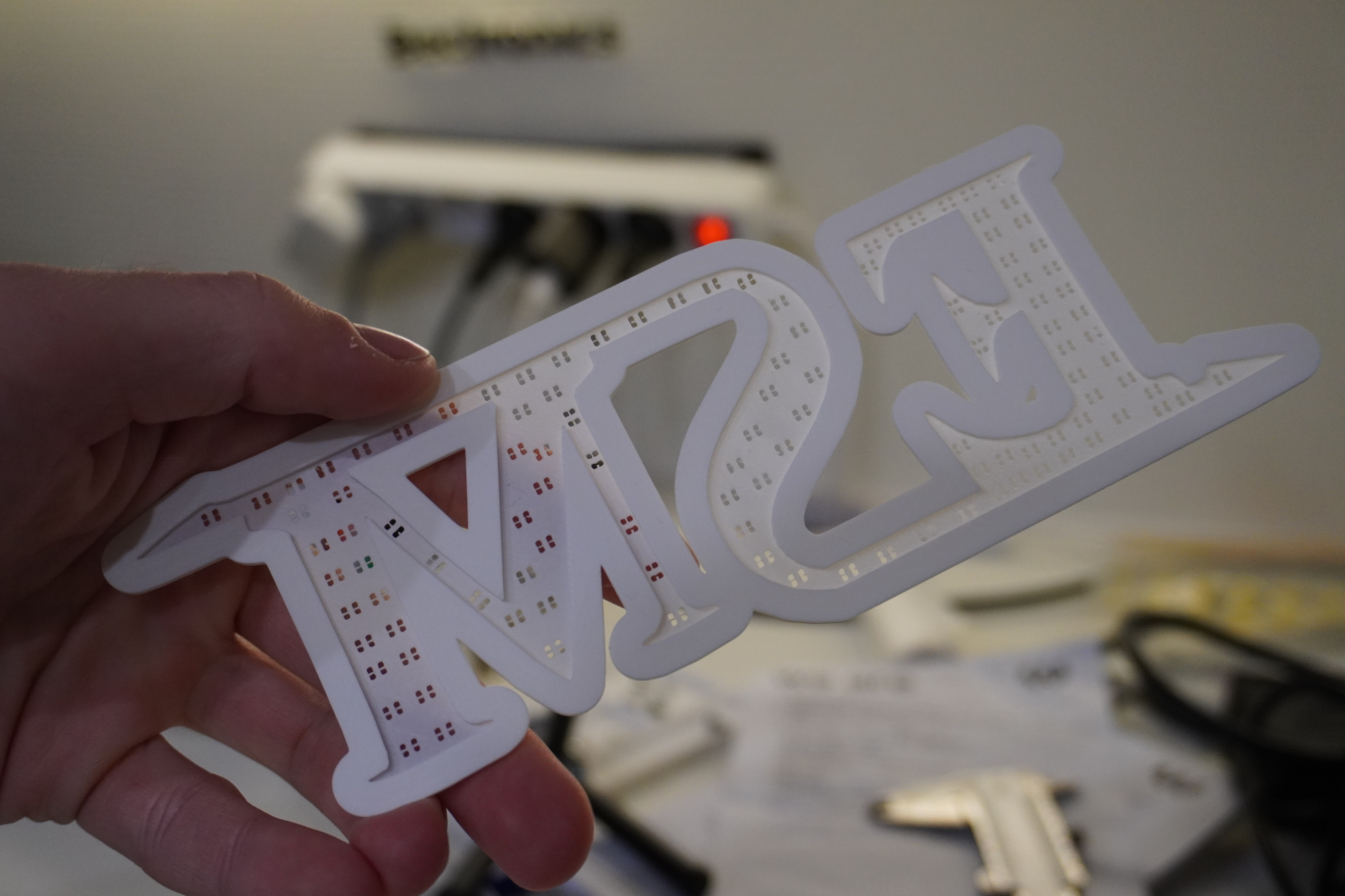
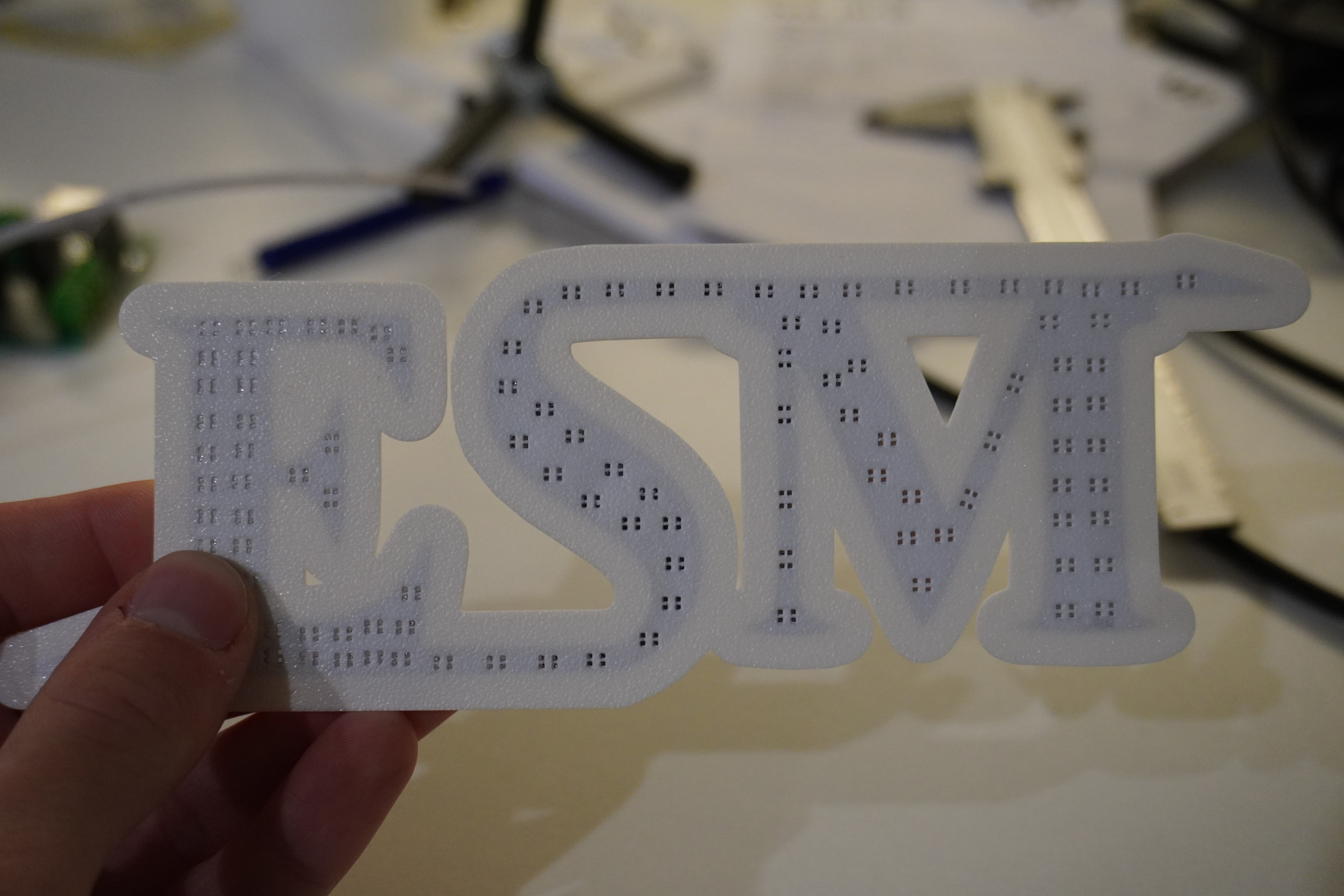 I guess I found my new workflow to solder SMD boards at home!
If you want the guide by kikit: https://yaqwsx.github.io/KiKit/latest/stencil/